© ROOT-NATION.com - Use of content is permitted with a backlink.
Today, we will talk about the transistors of the future and reveal all the secrets of their creation. It is already clear that ahead of us lies a period of immense changes in the structure and production methods of chips, which the market has not seen for a long time. The world’s brightest minds spend sleepless nights pondering which formula to use to make individual atoms dance just the way they need to and perform tasks that seem to defy the laws of physics.
This will also be a period of intensified competition among semiconductor giants from the USA, Korea, and Taiwan. They are the ones trying to capitalize on the future paradigm shift to regain, obtain, or strengthen their positions as technological leaders. What innovations and revolutions await us exactly? Let’s try to explain today.
Також читайте: What is AMD XDNA? Architecture that launches AI on Ryzen processors
Changing the transistor geometry
More precisely, their goals will change. The first innovation that will be (or has been!) introduced by the big three semiconductor manufacturers (TSMC, Intel, Samsung) is the so-called GAAFET transistors. This is the first significant change in transistor geometry since 2011 when the world saw Intel’s FinFET transistors. I don’t want to delve too much into the topic of GAAFET transistors because it requires a separate article. Here, we will only discuss the concept underlying them.

With the miniaturization of transistors, engineers began to experience what are known as short-channel effects. In short, as the distance between the source and drain of the transistor decreased, the problem became more pronounced. That is, the gate began to lose control over the current flowing through the channel. For decades, the solution to this problem involved making the channel protrude from the surface of the silicon wafer as a fin (hence Fin in FinFET). This allows the gate to make contact with the channel from three sides (or two if the fin has a wedge-shaped cross-section), providing greater control over the current flow and greater flexibility in adapting the electrical parameters of the transistors to the design requirements.
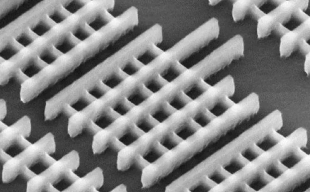 However, the continuous reduction in transistor size meant that this was no longer sufficient. It was necessary for the gate to start surrounding the transistor channel, forming GAAFET transistors (GAA stands for Gate-All-Around). Put simply, you can think of them as FinFET transistors placed side by side, as FinFET transistors often have two or three fins. It’s like a multi-level sandwich, where the channels in the form of tubes or sheets, stacked on top of each other, are separated by layers of insulator and gate. Although this concept has been known for many years and uses existing equipment and processes, its implementation is not trivial. The problem lies in the fact that at some stage, the subsequent layers of the channel hang in the air, supported only by a temporary “pillar”. At the same time, their lower part must be uniformly covered with a dielectric layer of a thickness of individual atoms, and then carefully filled with material to fill all the voids.

The fact that GAAFET transistors are not a trivial matter is underscored by Samsung’s situation. Since 2022, Samsung has had a process with MBCFET transistors (Samsung’s marketing name for implementing GAAFET transistors) in its portfolio. However, in practice, this is a typical Pyrrhic victory in the race. The percentage of fully functional chips obtained using it is so low that almost no one wants to use it in production (even… Samsung for its Exynos). All we know is that it is used for producing small and relatively simple microchips for cryptocurrency miners. It is expected that only the second generation of this process, which will be available in 2024 under the name 3GAP (although some sources say it could be renamed as a 2nm-class process), will be used more widely.

This year, GAAFET transistors (Intel calls its implementation RibbonFET) are expected to be delivered to Intel’s factories as part of the Intel 20A and 18A processes, which will be used for producing components for the Arrow Lake and Lunar Lake systems. However, various industry rumors suggest that initial production scales may be limited.
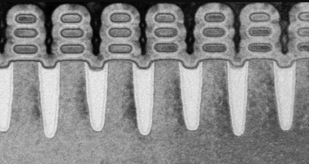
How about TSMC? The Taiwanese company plans to use GAAFET transistors in its N2 process, which is expected to be fully ready only by 2025. Theoretically later than Samsung and Intel, but when TSMC talks about the availability of a certain process, it usually means readiness to manufacture something for Apple and Nvidia, so in practice, the difference may be much smaller.
Read also: What’s new in Windows 11 Moment 5
The change in how transistors are powered.
The second innovation awaiting us is related to how transistors will be powered in microchips. Currently, the process of manufacturing a microprocessor occurs layer by layer from bottom to top. Transistors are built at the bottom, then interconnect networks are built above them, and then power cables are added. Typically, there are from a dozen to over twenty layers, and the higher the layer, the larger its elements.
Over the next few years, the standard will be that after creating connections between transistors, the silicon wafer will be flipped, thinned, and the power lines will be created on the other, polished side of the wafer. This means that the transistors will be like a patty in a burger, rather than being the base of a cake.
 It’s easy to imagine how this will complicate the process of manufacturing microchips, but according to initial experiments, the Back Side Power Delivery Network (BSPDN) brings many benefits. Firstly, with this approach, transistors can be placed closer to each other. Secondly, the overall number of layers will be reduced. Thirdly, the connections from the highest level of power source to the transistor will be shorter. This means lower energy losses and the potential for reducing the supply voltage. The exact methods of implementing this solution may vary in complexity and potential advantages, but all the major players in the market say it’s worth working on.

Later this year, we will see the BSPDN in action for the first time in the Intel Process 20A (Intel calls its implementation PowerVia). This rapid development is owed to the fact that Intel has been working on this technology for some time, independently of the work on changing transistor geometry and using newer machinery. This means that they will be able to integrate it practically into any future process.
Samsung has not yet provided any official information regarding when it will start using its version of the BSPDN backside power delivery network process. There’s not much news, but we know that Intel is already experimenting with this solution. Industry rumors suggest the possibility of its implementation in the SF2 process, scheduled for 2025, or in the next one planned for 2027.
TSMC is also taking its time in this area, reporting that while initial experiments yield promising results, it intends to introduce BSPDN into the N2P process, scheduled for implementation only at the intersection of 2026 and 2027.
Read also: Highlights of #MWC2024: Vision of the Future of Electronics World
Change of plate exposure machines
There is no serious discussion about microprocessor manufacturing without mentioning the Rayleigh criterion. In the case of lithography, which refers to the process of exposing silicon wafers, it takes the form of the following formula:
CD = k1 • λ / NA
In simpler terms, this means that the size of the smallest element that can be created by light on the surface of a silicon wafer depends on three factors:
k1 – a dimensionless coefficient in practice, indicating the effectiveness of the process;
λ – the wavelength of the light illuminating the wafer;
NA – the numerical aperture of the optical system.
For many years, the primary method of increasing transistor packing density was to use light with progressively shorter wavelengths. We started with wavelengths in the range of several hundred nanometers and relatively quickly moved to using light with a wavelength of 193 nm, on which semiconductor lithography got stuck much longer than expected. After years of research, delays, and billions of dollars spent, in 2019, ASML’s extreme ultraviolet lithography (EUV) machines finally hit the market. They use EUV light with a wavelength of approximately 13.5 nm and are now deployed in all advanced semiconductor manufacturing plants. However, this is likely the last time that λ could be reduced in the formula mentioned above.
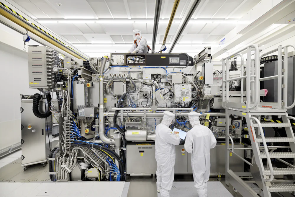
That’s why we’ll have to play around with changing NA. NA can be thought of as the aperture of a camera lens. This dimensionless number determines how much light the optical system collects. In the case of lithographic machines, this means (according to the formula mentioned above) that if we want to create smaller and smaller features, NA must be higher. The ASML machines currently in use have an NA of 0.33. The next step is machines with a high numerical aperture optical system, which have an NA of 0.55.
It sounds simple, but in this business, there’s nothing easy. This is best evidenced by the fact that High-NA machines are much larger and more than twice as expensive as their predecessors (around $400 million compared to approximately $150 million), while having lower throughput. Therefore, although everyone knows that this is the future of manufacturing the most advanced processors, it is often perceived as a necessary evil.
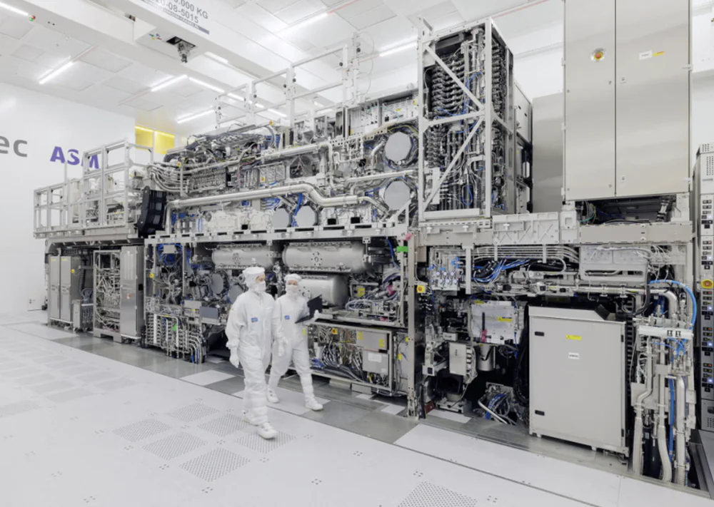 Intel has been the quickest to adopt the use of High-NA EUV machines. The American company has already acquired the first available machine of this type, which is currently being installed at one of its facilities in Oregon. Additionally, Intel plans to purchase the majority of machines manufactured this year. Developers are known to intend to use High-NA lithography on a large scale in the 14A process, expected to debut in 2026 or 2027 (if all goes according to plan).

Meanwhile, Samsung and TSMC are not rushing, hesitating about the economic sense of using this equipment until the implementation of the 1-nm technology node, which is approximately around 2030. Instead, they intend to squeeze out all possible benefits from the EUV machines they already possess through various tricks and process enhancements falling under the umbrella of the k1 coefficient.
Read also: How Taiwan, China and the US are fighting for technological dominance: the great chip war
Transition to 3D
Currently, we are entering the realm of the uncertain future, research works, and general assumptions rather than specific plans. However, the community is united in the belief that there will come a time when transistors need to be stacked on top of each other, as scaling along the X and Y axes is nearing its limit. Currently, P-type and N-type transistors are placed next to each other. The goal is to stack N-type transistors on top of P-type transistors, thus creating “sandwiches” of transistors known as CFETs (Complementary FETs). Two main methods are being explored to achieve this construction: monolithic, where the entire structure is built on one wafer, and sequential, where N- and P-type transistors are fabricated on separate wafers that are “bonded” together.
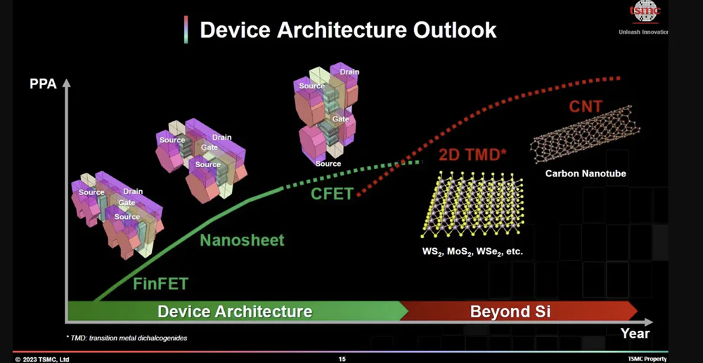
According to experts’ estimates, the microprocessor manufacturing market will enter the third dimension around 2032-2034. Currently, it is known that Intel and TSMC are actively working on their implementations of this technology, but Samsung is also likely not idle, as the potential benefits of using this solution are enormous.
Read alsо: Neuralink Telepathy chip: what it is and how it works
Transition to “two dimensions”
Another issue that world leaders in chip manufacturing are trying to address is the simple fact that there is a shortage of silicon. This element has served us faithfully for decades, but its limited supply is beginning to hinder the continued production of smaller and faster transistors. Therefore, research into so-called two-dimensional materials that could replace silicon in the transistor channel is ongoing worldwide. These materials have thicknesses of just a few atoms or even just one atom, providing electrical charge mobility that is inaccessible to silicon semiconductors of such thickness.

Graphene, as a two-dimensional material, has numerous potential applications, including semiconductor component manufacturing. However, its use in chip production still requires further research and development due to certain technical challenges, notably the lack of a bandgap. Nevertheless, Transition Metal Dichalcogenides (TMDs) such as MoS2 and WSe2 are more promising for semiconductor manufacturing due to their unique electronic properties. Research being conducted by Intel and TSMC in this direction could lead to significant discoveries and the development of new technologies in the next decade.
Read also: Midjourney V6: all about the next generation of AI
Interesting times ahead
To summarize, the next few years will be filled with innovations and revolutions in the semiconductor industry. The innovations described above do not even exhaust the topic, because we have not mentioned anything about computer lithography, chip development, or the potential transition to Glass processors. We also did not talk about progress in memory production.
Everyone knows that such pivotal moments are ideal for catching up technologically, as there is a high likelihood of competitors failing. Intel has even staked the future of the company on its ability to offer the next semiconductor innovations faster than its competitors. The U.S. government is also highly interested in bringing advanced chip manufacturing back to North America, hence it is investing billions of dollars in Intel’s developments. However, chip subsidies are not just a matter of interest for Americans. In Korea and Taiwan, governments also provide generous incentives to Samsung and TSMC, knowing how crucial the future period is and how much the future of these countries depends on new technologies. Among other reasons, this is because they have China behind them, which is also investing huge sums in semiconductor research, development, and production, but that is a topic for another article.
Read also:

